As of late January 2026, the artificial intelligence industry finds itself in a familiar yet intensified paradox: despite a historic, multi-billion-dollar expansion of semiconductor manufacturing capacity, the "Compute Crunch" remains the defining characteristic of the tech landscape. At the heart of this struggle is Taiwan Semiconductor Manufacturing Co. (TPE: 2330) and its Chip-on-Wafer-on-Substrate (CoWoS) advanced packaging technology. While TSMC has successfully quadrupled its CoWoS output compared to late 2024 levels, the insatiable hunger of generative AI models has kept the supply chain in a state of perpetual "catch-up," making advanced packaging the ultimate gatekeeper of global AI progress.
This persistent bottleneck is the physical manifestation of Item 9 on our Top 25 AI Developments list: The Infrastructure Ceiling. As AI models shift from the trillion-parameter Blackwell era into the multi-trillion-parameter Rubin era, the limiting factor is no longer just how many transistors can be etched onto a wafer, but how many high-bandwidth memory (HBM) modules and logic dies can be fused together into a single, high-performance package.
The Technical Frontier: Beyond Simple Silicon
The current state of CoWoS in early 2026 is a far cry from the nascent stages of two years ago. TSMC’s AP6 facility in Zhunan is now operating at peak capacity, serving as the workhorse for NVIDIA's (NASDAQ: NVDA) Blackwell series. However, the technical specifications have evolved. We are now seeing the widespread adoption of CoWoS-L, which utilizes local silicon interconnects (LSI) to bridge chips, allowing for larger package sizes that exceed the traditional "reticle limit" of a single chip.
Technical experts point out that the integration of HBM4—the latest generation of High Bandwidth Memory—has added a new layer of complexity. Unlike previous iterations, HBM4 requires a more intricate 2048-bit interface, necessitating the precision that only TSMC’s advanced packaging can provide. This transition has rendered older "on-substrate" methods obsolete for top-tier AI training, forcing the entire industry to compete for the same limited CoWoS-L and SoIC (System on Integrated Chips) lines. The industry reaction has been one of cautious awe; while the throughput of these packages is unprecedented, the yields for such complex "chiplets" remain a closely guarded secret, frequently cited as the reason for the continued delivery delays of enterprise-grade AI servers.
The Competitive Arena: Winners, Losers, and the Arizona Pivot
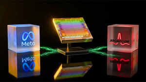
The scarcity of CoWoS capacity has created a rigid hierarchy in the tech sector. NVIDIA remains the undisputed king of the queue, reportedly securing nearly 60% of TSMC’s total 2026 capacity to fuel its transition to the Rubin (R100) architecture. This has left rivals like AMD (NASDAQ: AMD) and custom silicon giants like Broadcom (NASDAQ: AVGO) and Marvell Technology (NASDAQ: MRVL) in a fierce battle for the remaining slots. For hyperscalers like Google and Amazon, who are increasingly designing their own AI accelerators (TPUs and Trainium), the CoWoS bottleneck represents a strategic risk that has forced them to diversify their packaging partners.
To mitigate this, a landmark collaboration has emerged between TSMC and Amkor Technology (NASDAQ: AMKR). In a strategic move to satisfy U.S. "chips-act" requirements and provide geographical redundancy, the two firms have established a turnkey advanced packaging line in Peoria, Arizona. This allows TSMC to perform the front-end "Chip-on-Wafer" process in its Phoenix fabs while Amkor handles the "on-Substrate" finishing nearby. While this has provided a pressure valve for North American customers, it has not yet solved the global shortage, as the most advanced "Phase 1" of TSMC’s massive AP7 plant in Chiayi, Taiwan, has faced minor delays, only just beginning its equipment move-in this quarter.
A Wider Significance: Packaging is the New Moore’s Law
The CoWoS saga underscores a fundamental shift in the semiconductor industry. For decades, progress was measured by the shrinking size of transistors. Today, that progress has shifted to "More than Moore" scaling—using advanced packaging to stack and stitch together multiple chips. This is why advanced packaging is now a primary revenue driver, expected to contribute over 10% of TSMC’s total revenue by the end of 2026.
However, this shift brings significant geopolitical and environmental concerns. The concentration of advanced packaging in Taiwan remains a point of vulnerability for the global AI economy. Furthermore, the immense power requirements of these multi-die packages—some consuming over 1,000 watts per unit—have pushed data center cooling technologies to their limits. Comparisons are often drawn to the early days of the jet engine: we have the power to reach incredible speeds, but the "materials science" of the engine (the package) is now the primary constraint on how fast we can go.
The Road Ahead: Panel-Level Packaging and Beyond
Looking toward the horizon of 2027 and 2028, TSMC is already preparing for the successor to CoWoS: CoPoS (Chip-on-Panel-on-Substrate). By moving from circular silicon wafers to large rectangular glass panels, TSMC aims to increase the area of the packaging surface by several multiples, allowing for even larger "AI Super-Chips." Experts predict this will be necessary to support the "Rubin Ultra" chips expected in late 2027, which are rumored to feature even more HBM stacks than the current Blackwell-Ultra configurations.
The challenge remains the "yield-to-complexity" ratio. As packages become larger and more complex, the chance of a single defect ruining a multi-thousand-dollar assembly increases. The industry is watching closely to see if TSMC’s Arizona AP1 facility, slated for construction in the second half of this year, can replicate the high yields of its Taiwanese counterparts—a feat that has historically proven difficult.
Wrapping Up: The Infrastructure Ceiling
In summary, TSMC’s Herculean efforts to ramp CoWoS capacity to 120,000+ wafers per month by early 2026 are a testament to the company's engineering prowess, yet they remain insufficient against the backdrop of the global AI gold rush. The bottleneck has shifted from "can we make the chip?" to "can we package the system?" This reality cements Item 9—The Infrastructure Ceiling—as the most critical challenge for AI developers today.
As we move through 2026, the key indicators to watch will be the operational ramp of the Chiayi AP7 plant and the success of the Amkor-TSMC Arizona partnership. For now, the AI industry remains strapped to the pace of TSMC’s cleanrooms. The long-term impact is clear: those who control the packaging, control the future of artificial intelligence.
This content is intended for informational purposes only and represents analysis of current AI developments.
TokenRing AI delivers enterprise-grade solutions for multi-agent AI workflow orchestration, AI-powered development tools, and seamless remote collaboration platforms.
For more information, visit https://www.tokenring.ai/.