As the artificial intelligence revolution enters its most demanding phase in 2026, the semiconductor industry has reached a pivotal turning point. The traditional methods of powering microchips—which have remained largely unchanged for decades—are being discarded in favor of a radical new architecture known as Backside Power Delivery (BSPDN). This shift is not merely an incremental upgrade; it is a fundamental redesign of the silicon wafer that is proving to be the "secret weapon" for the next generation of sub-2nm AI processors.
By moving the complex network of power delivery lines from the top of the silicon wafer to its underside, chipmakers are finally breaking the "power wall" that has threatened to stall Moore’s Law. This innovation, spearheaded by industry giants Intel and TSMC, allows for significantly higher power efficiency, reduced signal interference, and a dramatic increase in logic density. For the AI industry, which is currently grappling with the immense energy demands of trillion-parameter models, BSPDN is the critical infrastructure enabling the hardware of tomorrow.
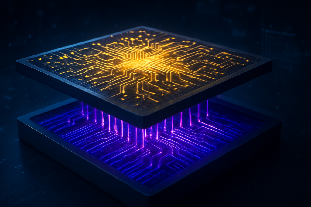
The Great Flip: Moving Power to the Backside
The technical transition to Backside Power Delivery represents the most significant architectural change in chip manufacturing since the introduction of FinFET transistors. Historically, both power and data signals were routed through a dense "forest" of metal layers on the front side of the wafer. As transistors shrank to the 2nm level and below, this "Front-side Power Delivery" (FSPDN) became a major bottleneck. The power lines and signal lines competed for the same limited space, leading to "IR drop"—a phenomenon where voltage is lost to resistance before it even reaches the transistors—and signal interference that hampered performance.
Intel Corporation (NASDAQ: INTC) was the first to cross the finish line with its implementation, branded as PowerVia. Integrated into the Intel 18A (1.8nm) node, PowerVia utilizes Nano-Through Silicon Vias (nTSVs) to deliver electricity directly to the transistors from the back. This approach has already demonstrated a 30% reduction in IR droop and a roughly 6% increase in frequency at iso-power. Meanwhile, Taiwan Semiconductor Manufacturing Co. (NYSE: TSM) is preparing its Super Power Rail technology for the A16 node. Unlike Intel’s nTSVs, TSMC’s implementation uses direct contact to the source and drain, which is more complex to manufacture but promises an 8–10% speed improvement and up to 20% power reduction compared to its previous N2P node.
The reaction from the AI research and hardware communities has been overwhelmingly positive. Experts note that while previous node transitions focused on making transistors smaller, BSPDN focuses on making them more accessible. By clearing the "congestion" on the front side of the chip, designers can now pack more logic gates and High Bandwidth Memory (HBM) interconnects into the same physical area. This "unclogging" of the chip's architecture is what allows for the extreme density required by the latest AI accelerators.
A New Competitive Landscape for AI Giants
The arrival of BSPDN has sparked a strategic reshuffling among the world’s most valuable tech companies. Intel’s early success with PowerVia has allowed it to secure major foundry customers who were previously exclusive to TSMC. Microsoft (NASDAQ: MSFT), for instance, has become a lead customer for Intel’s 18A process, utilizing it for its Maia 3 AI accelerators. For Microsoft, the power efficiency gains of BSPDN are vital for managing the astronomical electricity costs of its global data center footprint.
TSMC, however, remains the dominant force in the high-end AI market. While its A16 node is not scheduled for high-volume manufacturing until the second half of 2026, NVIDIA (NASDAQ: NVDA) has reportedly secured early access for its upcoming "Feynman" architecture. NVIDIA’s current Blackwell successors already push the limits of thermal design power (TDP), often exceeding 1,000 watts. The Super Power Rail technology in A16 is seen as the only viable path to sustaining the performance leaps NVIDIA needs for its 2027 and 2028 roadmaps.
Even Apple (NASDAQ: AAPL), which has long been TSMC’s most loyal partner, is reportedly exploring diversification. While Apple is expected to use TSMC’s N2P for the iPhone 18 Pro in late 2026, rumors suggest the company is qualifying Intel’s 18A for its entry-level M-series chips in 2027. This shift highlights how critical BSPDN has become; the competitive advantage is no longer just about who has the smallest transistors, but who can power them most efficiently.
Breaking the Power Wall and Enabling 3D Silicon
The broader significance of Backside Power Delivery lies in its ability to solve the thermal and energy crises currently facing the AI landscape. As AI models grow, the chips that train them require more current. In a traditional design, the heat generated by power delivery on the front side of the chip sits directly on top of the heat-generating transistors, creating a "thermal sandwich" that is difficult to cool. By moving power to the backside, the front of the chip can be more effectively cooled by direct-contact liquid cooling or advanced heat sinks.
This architectural shift also paves the way for advanced 3D-stacked chips. In a 3D configuration, multiple layers of logic and memory are piled on top of each other. Previously, getting power to the middle layers of such a stack was a logistical nightmare. BSPDN provides a blueprint for "sandwiching" power and cooling between logic layers, which many believe is the only way to eventually achieve "brain-scale" computing.
However, the transition is not without its concerns. The manufacturing process for BSPDN requires extreme wafer thinning—grinding the silicon down to just a few micrometers—and complex wafer-to-wafer bonding. This increases the risk of manufacturing defects and could lead to higher initial costs for AI startups. There is also the concern of "vendor lock-in," as the design tools required for Intel’s PowerVia and TSMC’s Super Power Rail are not fully interchangeable, forcing chip designers to choose a side early in the development cycle.
The Road to 1nm and Beyond
Looking ahead, the successful deployment of BSPDN in 2026 is just the beginning. Experts predict that by 2028, backside power will be standard across all high-performance computing (HPC) and mobile chips. The next frontier will be the integration of optical interconnects directly onto the backside of the wafer, allowing chips to communicate via light rather than electricity, further reducing heat and increasing bandwidth.
In the near term, the industry is watching the H2 2026 ramp-up of TSMC’s A16 node. If TSMC can achieve high yields quickly, it could accelerate the release of OpenAI’s rumored custom "XPU" (eXtreme Processing Unit), which is being designed in collaboration with Broadcom (NASDAQ: AVGO) to leverage Super Power Rail for GPT-6 training clusters. The challenge remains the sheer complexity of the manufacturing process, but the rewards—chips that are 20% faster and significantly cooler—are too great for any major player to ignore.
A Milestone in Semiconductor History
Backside Power Delivery marks the end of the "two-dimensional" era of chip design and the beginning of a truly three-dimensional future. By decoupling the delivery of energy from the processing of data, Intel and TSMC have provided the AI industry with a new lease on life. This development will likely be remembered as the moment when the physical limits of silicon were pushed back, allowing the exponential growth of artificial intelligence to continue unabated.
As we move through 2026, the key metrics to watch will be the production yields of TSMC’s A16 and the real-world performance of Intel’s 18A-based server chips. For the first time in years, the "how" of chip manufacturing is just as important as the "how small." The secret weapon for sub-2nm efficiency is no longer a secret—it is the new foundation of the digital world.
This content is intended for informational purposes only and represents analysis of current AI developments.
TokenRing AI delivers enterprise-grade solutions for multi-agent AI workflow orchestration, AI-powered development tools, and seamless remote collaboration platforms.
For more information, visit https://www.tokenring.ai/.