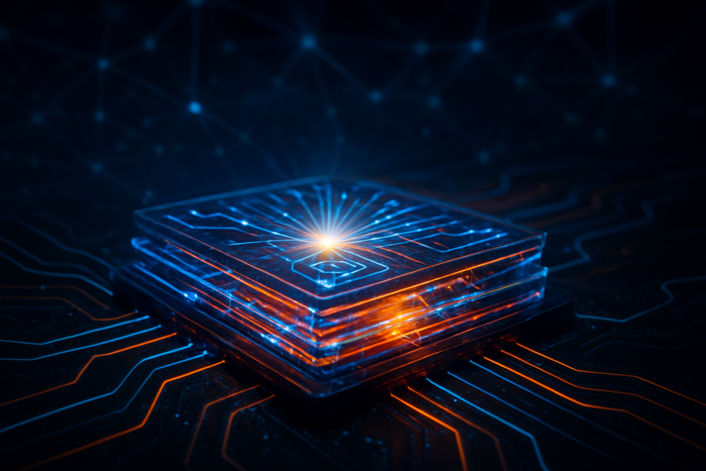
The artificial intelligence industry has officially entered the era of light-speed computing. At the conclusion of CES 2026, it has become clear that the "Copper Wall"—the physical limit where traditional electrical wiring can no longer transport data between chips without melting under its own heat or losing signal integrity—has finally been breached. The solution, long-promised but now finally at scale, is Silicon Photonics (SiPh) and Co-Packaged Optics (CPO). By integrating laser-based communication directly into the chip package, the industry is overcoming the energy and latency bottlenecks that threatened to stall the development of trillion-parameter AI models.
This month's announcements from industry titans and specialized startups mark a paradigm shift in how AI supercomputers are built. Instead of massive clusters of GPUs struggling to communicate over meters of copper cable, the new "Optical AI Factory" uses light to move data with a fraction of the energy and virtually no latency. As NVIDIA (NASDAQ: NVDA) and Broadcom (NASDAQ: AVGO) move into volume production of CPO-integrated hardware, the blueprint for the next generation of AI infrastructure has been rewritten in photons.
At the heart of this transition is the move from "pluggable" optics—the removable modules that have sat at the edge of servers for decades—to Co-Packaged Optics (CPO). In a CPO architecture, the optical engine is moved directly onto the same substrate as the GPU or network switch. This eliminates the power-hungry Digital Signal Processors (DSPs) and long copper traces previously required to drive electrical signals across a circuit board. At CES 2026, NVIDIA unveiled its Spectrum-6 Ethernet Switch (SN6800), which delivers a staggering 409.6 Tbps of aggregate bandwidth. By utilizing integrated silicon photonic engines, the Spectrum-6 reduces interconnect power consumption by 5x compared to the previous generation, while simultaneously increasing network resiliency by an order of magnitude.
Technical specifications for 2026 hardware show a massive leap in energy efficiency, measured in picojoules per bit (pJ/bit). Traditional copper and pluggable systems in early 2025 typically consumed 12–15 pJ/bit. The new CPO systems from Broadcom—specifically the Tomahawk 6 "Davisson" switch, now in full volume production—have driven this down to less than 3.8 pJ/bit. This 70% reduction in power is not merely an incremental improvement; it is the difference between an AI data center requiring a dedicated nuclear power plant or fitting within existing power grids. Furthermore, latency has plummeted. While pluggable optics once added 100–600 nanoseconds of delay, new optical I/O solutions from startups like Ayar Labs are demonstrating near-die speeds of 5–20 nanoseconds, allowing thousands of GPUs to function as one cohesive, massive brain.
This shift differs from previous approaches by moving light generation and modulation from the "shoreline" (the edge of the chip) into the heart of the package using 3D-stacking. TSMC (NYSE: TSM) has been instrumental here, moving its COUPE (Compact Universal Photonics Engine) technology into mass production. Using SoIC-X (System on Integrated Chips), TSMC is now hybrid-bonding electronic dies directly onto silicon photonics dies. The AI research community has reacted with overwhelming optimism, as these specifications suggest that the "communication overhead" which previously ate up 30-50% of AI training cycles could be virtually eliminated by the end of 2026.
The commercial implications of this breakthrough are reorganizing the competitive landscape of Silicon Valley. NVIDIA (NASDAQ: NVDA) remains the frontrunner, using its Rubin GPU architecture—officially launched this month—to lock customers into a vertically integrated optical ecosystem. By combining its Vera CPUs and Rubin GPUs with CPO-based NVLink fabrics, NVIDIA is positioning itself as the only provider capable of delivering a "turnkey" million-GPU cluster. However, the move to optics has also opened the door for a powerful counter-coalition.
Marvell (NASDAQ: MRVL) has emerged as a formidable challenger following its strategic acquisition of Celestial AI and XConn Technologies. By championing the UALink (Universal Accelerator Link) and CXL 3.1 standards, Marvell is providing an "open" optical fabric that allows hyperscalers like Amazon (NASDAQ: AMZN) and Google (NASDAQ: GOOGL) to build custom AI accelerators that can still compete with NVIDIA’s performance. The strategic advantage has shifted toward companies that control the packaging and the silicon photonics IP; as a result, TSMC (NYSE: TSM) has become the industry's ultimate kingmaker, as its CoWoS and SoIC packaging capacity now dictates the total global supply of CPO-enabled AI chips.
For startups and secondary players, the barrier to entry has risen significantly. The transition to CPO requires advanced liquid cooling as a default standard, as integrated optical engines are highly sensitive to the massive heat generated by 1,200W GPUs. Companies that cannot master the intersection of photonics, 3D packaging, and liquid cooling are finding themselves sidelined. Meanwhile, the pluggable transceiver market—once a multi-billion dollar stronghold for traditional networking firms—is facing a rapid decline as Tier-1 AI labs move toward fixed, co-packaged solutions to maximize efficiency and minimize total cost of ownership (TCO).
The wider significance of silicon photonics extends beyond mere speed; it is the primary solution to the "Energy Wall" that has become a matter of national security and environmental urgency. As AI clusters scale toward power draws of 500 megawatts and beyond, the move to optics represents the most significant sustainability milestone in the history of computing. By reducing the energy required for data movement by 70%, the industry is effectively "recycling" that power back into actual computation, allowing for larger models and faster training without a proportional increase in carbon footprint.
Furthermore, this development marks the decoupling of compute from physical distance. In traditional copper-based architectures, GPUs had to be packed tightly together to maintain signal integrity, leading to extreme thermal densities. Silicon photonics allows for data to travel kilometers with negligible loss, enabling "Disaggregated Data Centers." In this new model, memory, compute, and storage can be located in different parts of a facility—or even different buildings—while still performing as if they were on the same motherboard. This is a fundamental break from the Von Neumann architecture constraints that have defined computing for 80 years.
However, the transition is not without concerns. The move to CPO creates a "repairability crisis" in the data center. Unlike pluggable modules, which can be easily swapped if they fail, a failed optical engine in a CPO system may require replacing an entire $40,000 GPU or a $200,000 switch. To combat this, NVIDIA and Broadcom have introduced "detachable fiber connectors" and external laser sources (ELS), but the long-term reliability of these integrated systems in the 24/7 high-heat environment of an AI factory remains a point of intense scrutiny among industry skeptics.
Looking ahead, the near-term roadmap for silicon photonics is focused on "Optical Memory." Marvell and Celestial AI have already demonstrated optical memory appliances that provide up to 33TB of shared capacity with sub-200ns latency. This suggests that by late 2026 or 2027, the concept of "GPU memory" may become obsolete, replaced by a massive, shared pool of HBM4 memory accessible by any processor in the rack via light. We also expect to see the debut of 1.6T and 3.2T per-port speeds as 200G-per-lane SerDes become the standard.
Long-term, experts predict the arrival of "All-Optical Computing," where light is used not just for moving data, but for the actual mathematical operations within the Tensor cores. While this remains in the lab stage, the successful commercialization of CPO is the necessary first step. The primary challenge over the next 18 months will be manufacturing yield. As photonics moves into the 3D-stacking realm, the complexity of bonding light-emitting materials with silicon is immense. Predictably, the industry will see a "yield war" as foundries race to stabilize the production of these complex multi-die systems.
The arrival of Silicon Photonics and Co-Packaged Optics in early 2026 represents a "point of no return" for the AI industry. The transition from electrical to optical interconnects is perhaps the most significant hardware breakthrough since the invention of the integrated circuit, effectively removing the physical boundaries that limited the scale of artificial intelligence. With NVIDIA's Rubin platform and Broadcom's Davisson switches now leading the charge, the path to million-GPU clusters is no longer blocked by the "Copper Wall."
The key takeaway is that the future of AI is no longer just about the number of transistors on a chip, but the number of photons moving between them. This development ensures that the rapid pace of AI advancement can continue through the end of the decade, supported by a new foundation of energy-efficient, low-latency light-speed networking. In the coming months, the industry will be watching the first deployments of the Rubin NVL72 systems to see if the real-world performance matches the spectacular benchmarks seen at CES. For now, the era of "Computing at the Speed of Light" has officially dawned.
This content is intended for informational purposes only and represents analysis of current AI developments.
TokenRing AI delivers enterprise-grade solutions for multi-agent AI workflow orchestration, AI-powered development tools, and seamless remote collaboration platforms.
For more information, visit https://www.tokenring.ai/.