The foundational material of the digital age, silicon, is encountering its inherent physical limits, prompting a pivotal shift in semiconductor manufacturing. While Silicon Carbide (SiC) has rapidly emerged as a dominant force in high-power applications, a new wave of advanced materials is now poised to redefine the very essence of microchip performance and unlock unprecedented capabilities across various industries. This evolution signifies more than an incremental upgrade; it represents a fundamental re-imagining of how electronic devices are built, promising to power the next generation of artificial intelligence, electric vehicles, and beyond.
This paradigm shift is driven by an escalating demand for chips that can operate at higher frequencies, withstand extreme temperatures, consume less power, and deliver greater efficiency than what traditional silicon can offer. The exploration of materials like Gallium Nitride (GaN), Diamond, Gallium Oxide (Ga₂O₃), and a diverse array of 2D materials promises to overcome current performance bottlenecks, extend the boundaries of Moore's Law, and catalyze a new era of innovation in computing and electronics.
Unpacking the Technical Revolution: A Deeper Dive into Next-Gen Substrates
The limitations of silicon, particularly its bandgap and thermal conductivity, have spurred intensive research into alternative materials with superior electronic and thermal properties. Among the most prominent emerging contenders are wide bandgap (WBG) and ultra-wide bandgap (UWBG) semiconductors, alongside novel 2D materials, each offering distinct advantages that silicon struggles to match.
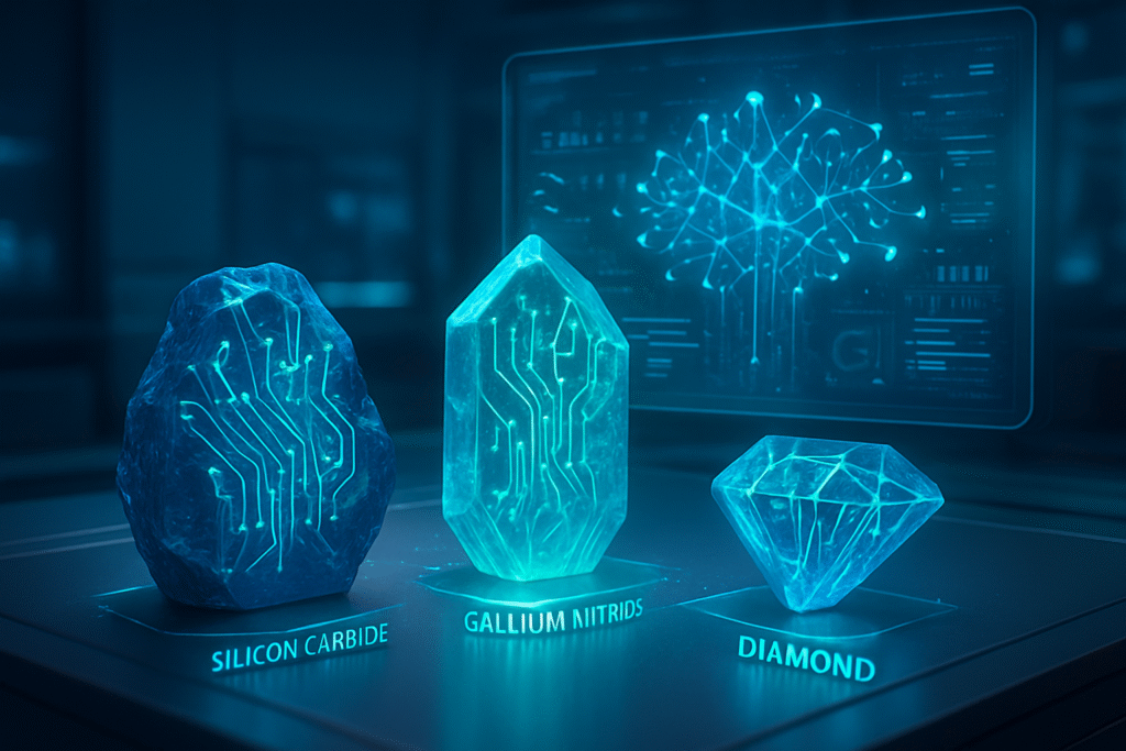
Gallium Nitride (GaN), already achieving commercial prominence, is a wide bandgap semiconductor (3.4 eV) excelling in high-frequency and high-power applications. Its superior electron mobility and saturation drift velocity allow for faster switching speeds and reduced power loss, making it ideal for power converters, 5G base stations, and radar systems. This directly contrasts with silicon's lower bandgap (1.12 eV), which limits its high-frequency performance and necessitates larger components to manage heat.
Diamond, an ultra-wide bandgap material (>5.5 eV), is emerging as a "game-changing contender" for extreme environments. Its unparalleled thermal conductivity (approximately 2200 W/m·K compared to silicon's 150 W/m·K) and exceptionally high breakdown electric field (30 times higher than silicon, 3 times higher than SiC) position it for ultra-high-power and high-temperature applications where even SiC might fall short. Researchers are also keenly investigating Gallium Oxide (Ga₂O₃), specifically beta-gallium oxide (β-Ga₂O₃), another UWBG material with significant potential for high-power devices due to its excellent breakdown strength.
Beyond these, 2D materials like graphene, molybdenum disulfide (MoS₂), and hexagonal boron nitride (h-BN) are being explored for their atomically thin structures and tunable properties. These materials offer avenues for novel transistor designs, flexible electronics, and even quantum computing, allowing for devices with unprecedented miniaturization and functionality. Unlike bulk semiconductors, 2D materials present unique quantum mechanical properties that can be exploited for highly efficient and compact devices. Initial reactions from the AI research community and industry experts highlight the excitement around these materials' potential to enable more efficient AI accelerators, denser memory solutions, and more robust computing platforms, pushing past the thermal and power density constraints currently faced by silicon-based systems. The ability of these materials to operate at higher temperatures and voltages with lower energy losses fundamentally changes the design landscape for future electronics.
Corporate Crossroads: Reshaping the Semiconductor Industry
The transition to advanced semiconductor materials beyond silicon and SiC carries profound implications for major tech companies, established chip manufacturers, and agile startups alike. This shift is not merely about adopting new materials but about investing in new fabrication processes, design methodologies, and supply chains, creating both immense opportunities and competitive pressures.
Companies like Infineon Technologies AG (XTRA: IFX), STMicroelectronics N.V. (NYSE: STM), and ON Semiconductor Corporation (NASDAQ: ON) are already significant players in the SiC and GaN markets, and stand to benefit immensely from the continued expansion and diversification into other WBG and UWBG materials. Their early investments in R&D and manufacturing capacity for these materials give them a strategic advantage in capturing market share in high-growth sectors like electric vehicles, renewable energy, and data centers, all of which demand the superior performance these materials offer.
The competitive landscape is intensifying as traditional silicon foundries, such as Taiwan Semiconductor Manufacturing Company (TSMC) (NYSE: TSM) and Samsung Electronics Co., Ltd. (KRX: 005930), are also dedicating resources to developing processes for GaN and SiC, and are closely monitoring other emerging materials. Their ability to scale production will be crucial. Startups specializing in novel material synthesis, epitaxy, and device fabrication for diamond or Ga₂O₃, though currently smaller, could become acquisition targets or key partners for larger players seeking to integrate these cutting-edge technologies. For instance, companies like Akhan Semiconductor are pioneering diamond-based devices, demonstrating the disruptive potential of focused innovation.
This development could disrupt existing product lines for companies heavily reliant on silicon, forcing them to adapt or risk obsolescence in certain high-performance niches. The market positioning will increasingly favor companies that can master the complex manufacturing challenges of these new materials while simultaneously innovating in device design to leverage their unique properties. Strategic alliances, joint ventures, and significant R&D investments will be critical for maintaining competitive edge and navigating the evolving semiconductor landscape.
Broader Horizons: Impact on AI, IoT, and Beyond
The shift to advanced semiconductor materials represents a monumental milestone in the broader AI landscape, enabling breakthroughs that were previously unattainable with silicon. The enhanced performance, efficiency, and resilience offered by these materials are perfectly aligned with the escalating demands of modern AI, particularly in areas like high-performance computing (HPC), edge AI, and specialized AI accelerators.
The ability of GaN and SiC to handle higher power densities and switch faster directly translates to more efficient power delivery systems for AI data centers, reducing energy consumption and operational costs. For AI inferencing at the edge, where power budgets are tight and real-time processing is critical, these materials allow for smaller, more powerful, and more energy-efficient AI chips. Beyond these, materials like diamond and Ga₂O₃, with their extreme thermal stability and breakdown strength, could enable AI systems to operate in harsh industrial environments or even space, expanding the reach of AI applications into new frontiers. The development of 2D materials also holds promise for novel neuromorphic computing architectures, potentially mimicking the brain's efficiency more closely than current digital designs.
Potential concerns include the higher manufacturing costs and the nascent supply chains for some of these exotic materials, which could initially limit their widespread adoption compared to the mature silicon ecosystem. Scalability remains a challenge for materials like diamond and Ga₂O₃, requiring significant investment in research and infrastructure. However, the benefits in performance, energy efficiency, and operational longevity often outweigh the initial cost, especially in critical applications. This transition can be compared to the move from vacuum tubes to transistors or from germanium to silicon; each step unlocked new capabilities and defined subsequent eras of technological advancement. The current move beyond silicon is poised to have a similar, if not greater, transformative impact.
The Road Ahead: Anticipating Future Developments and Applications
The trajectory for advanced semiconductor materials points towards a future characterized by unprecedented performance and diverse applications. In the near term, we can expect continued refinement and cost reduction in GaN and SiC manufacturing, leading to their broader adoption across more consumer electronics, industrial power supplies, and electric vehicle models. The focus will be on improving yield, increasing wafer sizes, and developing more sophisticated device architectures to fully harness their properties.
Looking further ahead, research and development efforts will intensify on ultra-wide bandgap materials like diamond and Ga₂O₃. Experts predict that as manufacturing techniques mature, these materials will find niches in extremely high-power applications such as next-generation grid infrastructure, high-frequency radar, and potentially even in fusion energy systems. The inherent radiation hardness of diamond, for instance, makes it a prime candidate for electronics operating in hostile environments, including space missions and nuclear facilities.
For 2D materials, the horizon includes breakthroughs in flexible and transparent electronics, opening doors for wearable AI devices, smart surfaces, and entirely new human-computer interfaces. The integration of these materials into quantum computing architectures also remains a significant area of exploration, potentially enabling more stable and scalable qubits. Challenges that need to be addressed include developing cost-effective and scalable synthesis methods for high-quality single-crystal substrates, improving interface engineering between different materials, and establishing robust testing and reliability standards. Experts predict a future where hybrid semiconductor devices, leveraging the best properties of multiple materials, become commonplace, optimizing performance for specific application requirements.
Conclusion: A New Dawn for Semiconductors
The emergence of advanced materials beyond traditional silicon and the rapidly growing Silicon Carbide marks a pivotal moment in semiconductor history. This shift is not merely an evolutionary step but a revolutionary leap, promising to dismantle the performance ceilings imposed by silicon and unlock a new era of innovation. The superior bandgap, thermal conductivity, breakdown strength, and electron mobility of materials like Gallium Nitride, Diamond, Gallium Oxide, and 2D materials are set to redefine chip performance, enabling more powerful, efficient, and resilient electronic devices.
The key takeaways are clear: the semiconductor industry is diversifying its material foundation to meet the insatiable demands of AI, electric vehicles, 5G/6G, and other cutting-edge technologies. Companies that strategically invest in the research, development, and manufacturing of these advanced materials will gain significant competitive advantages. While challenges in cost, scalability, and manufacturing complexity remain, the potential benefits in performance and energy efficiency are too significant to ignore.
This development's significance in AI history cannot be overstated. It paves the way for AI systems that are faster, more energy-efficient, capable of operating in extreme conditions, and potentially more intelligent through novel computing architectures. In the coming weeks and months, watch for announcements regarding new material synthesis techniques, expanded manufacturing capacities, and the first wave of commercial products leveraging these truly next-generation semiconductors. The future of computing is no longer solely silicon-based; it is multi-material, high-performance, and incredibly exciting.
This content is intended for informational purposes only and represents analysis of current AI developments.
TokenRing AI delivers enterprise-grade solutions for multi-agent AI workflow orchestration, AI-powered development tools, and seamless remote collaboration platforms.
For more information, visit https://www.tokenring.ai/.