'H-Cube' applies advanced silicon interposer technology and hybrid-substrate structure, allowing efficient integration of 6 HBMs, as well as lower cost benefit
Samsung Electronics, a world leader in advanced semiconductor technology, today announced that it has developed Hybrid-Substrate Cube (H-Cube) technology, its latest 2.5D packaging solution specialized for semiconductors for HPC, AI, data center, and network products that require high-performance and large-area packaging technology.
This press release features multimedia. View the full release here: https://www.businesswire.com/news/home/20211110006481/en/
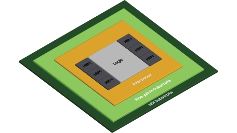
A top view of Samsung's new H-Cube packaging solution. (Graphic: Business Wire)
“H-Cube solution, which is jointly developed with Samsung Electro-mechanics (SEMCO) and Amkor Technology, is suited to high-performance semiconductors that need to integrate a large number of silicon dies,” said Moonsoo Kang, senior vice president and Head of Foundry Market Strategy Team at Samsung Electronics. “By expanding and enriching the foundry ecosystem, we will provide various package solutions to find a breakthrough in the challenges our customers are facing.”
“In today’s environment where system integration is increasingly required and substrate supplies are constrained, Samsung Foundry and Amkor Technology have successfully co-developed H-Cube to overcome these challenges,” said JinYoung Kim, senior vice president of Global R&D Center at Amkor Technology. “This development lowers barriers to entry in the HPC/AI market and demonstrates successful collaboration and partnership between the foundry and outsourced semiconductor assembly and test (OSAT) company.”
H-Cube Structure and Features
2.5D packaging enables logic chips or high-bandwidth memory (HBM) to be placed on top of a silicon interposer in a small form factor. Samsung’s H-Cube technology features a hybrid substrate combined with a fine-pitch substrate which is capable of fine bump connection, and a High-Density Interconnection (HDI) substrate, to implement large sizes into 2.5D packaging.
With the recent increase in specifications required in the HPC, AI, and networking application market segments, large-area packaging is becoming important as the number and size of chips mounted in one package increases or high-bandwidth communication is required. For attachment and connection of silicon dies including the interposer, fine-pitch substrates is essential but prices rise significantly following an increase in size.
When integrating six or more HBMs, the difficulty in manufacturing the large-area substrate increases rapidly, resulting in decreased efficiency. Samsung solved this problem by applying a hybrid substrate structure in which HDI substrates that are easy to implement in large-area is overlapped under a high-end fine-pitch substrate.
By decreasing the pitch of solder ball, which electrically connects the chip and the substrate, by 35% compared to the conventional ball pitch, the size of fine-pitch substrate can be minimized, while adding HDI substrate (module PCB) under the fine-pitch substrate to secure connectivity with the system board.
In addition, to enhance the reliability of the H-Cube solution, Samsung applied its proprietary signal/power integrity analysis technology that can stably supply power while minimizing the signal loss or distortion when stacking multiple logic chips and HBMs.
Looking ahead, in cooperation with its ecosystem partners, Samsung will hold its 3rd Annual ‘Samsung Advanced Foundry Ecosystem (SAFETM) Forum' virtually on November 17 (PST).
For pre-registration on the SAFE forum, please visit https://www.samsungfoundry.com
About Samsung Electronics Co., Ltd.
Samsung inspires the world and shapes the future with transformative ideas and technologies. The company is redefining the worlds of TVs, smartphones, wearable devices, tablets, digital appliances, network systems, and memory, system LSI, foundry and LED solutions. For the latest news, please visit the Samsung Newsroom at http://news.samsung.com.
View source version on businesswire.com: https://www.businesswire.com/news/home/20211110006481/en/
Contacts
Lisa Warren-Plungy
Samsung Semiconductor, Inc.
Lisa.plungy@samsung.com